
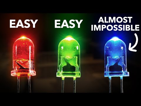
Veritasium • Why It Was Almost Impossible to Make the Blue LED
Content Summary
This report is generated from research on the following videos, based on the requirements set in Video Deep Research.
Analyze selected videos,
My goal is 📑 Discover Content Intelligence
My role is 📚 Student/Learner/Researcher
I need: 📖 Academic source validation and credibility check, 🤔 Knowledge gap identification, 🛤️ Learning pathway recommendations

https:...A41M
Summary
1. Navigating Institutional Skepticism and Industry Blind Spots
2. Overcoming Engineering Hurdles through Unconventional Material Selection
3. The Economic and Environmental Trajectory of Disruptive Technology
Knowledge Snap
Pathway 1: Foundational Materials Science
🎬 Related Clip
(3)
Video Title
00:00 - 00:15
The video outlines the basic physics of how semiconductors convert electrical energy into visible light particles.
00:00 - 00:15
A diagram shows the movement of electrons between different energy levels in a crystal lattice.
00:00 - 00:15
The researcher explains why some materials are naturally better suited for light emission than others.
Pathway 2: Intermediate Crystal Growth
🎬 Related Clip
(3)
Video Title
00:00 - 00:15
The narrator describes the high-pressure environment needed to grow high-quality gallium nitride crystals successfully.
00:00 - 00:15
Footage shows the specialized equipment used to deposit thin films of atoms onto sapphire surfaces.
00:00 - 00:15
An expert discusses the chemical reactions that take place inside a semiconductor manufacturing chamber.
Pathway 3: Advanced Photonic Engineering
🎬 Related Clip
(3)
Video Title
00:00 - 00:15
The video demonstrates how different layers of atoms are stacked to create a functional light-emitting diode.
00:00 - 00:15
A scientist explains how adding indium to the mix changes the color of the light emitted.
00:00 - 00:15
Thermal imaging shows how engineers manage the heat generated by high-intensity semiconductor devices.
Pathway 4: Research Validation Strategies
🎬 Related Clip
(3)
Video Title
00:00 - 00:15
The narrator notes that the scientific community initially refused to believe the reported success of the experiment.
00:00 - 00:15
Nakamura describes presenting his results at a conference where his data was met with complete silence.
00:00 - 00:15
The video explains how other laboratories eventually replicated the results to confirm the major discovery.
Pathway 5: Innovation and Patent Intelligence
🎬 Related Clip
(3)
Video Title
00:00 - 00:15
The narrator discusses the legal battles over the patents for the blue light emitting technology.
00:00 - 00:15
The video shows the rapid transition from a small-scale invention to a global manufacturing operation.
00:00 - 00:15
An expert explains why controlling the manufacturing process was as important as the original discovery.
Pathway 6: Interdisciplinary Sustainability Analysis
🎬 Related Clip
(3)
Video Title
00:00 - 00:15
Data visualizations show the dramatic drop in energy consumption following the adoption of newer light sources.
00:00 - 00:15
The narrator explores how the technology is now used in everything from smartphones to streetlights.
00:00 - 00:15
The video concludes by analyzing the potential for future improvements in lighting efficiency and color.
Evolution of High-Stakes Semiconductor Innovation
Why It Was Almost Impossible to Make the Blue LED
UCHnyfMqiRRG1u-2MsSQLbXA
🔍
Initial Technical Barriers
00:00 - 00:15
Researchers identify the massive gap in the visible light spectrum for diode technology.
📉
Academic Skepticism
00:00 - 00:15
Established experts reach a consensus that certain materials are not viable for production.
🧪
Material Science Challenges
00:00 - 00:15
Exploration into physical properties reveals significant engineering obstacles that discouraged many researchers.
💡
Persistence in Research
00:00 - 00:15
An unconventional path is chosen despite a lack of support from the broader scientific community.
🛠️
Engineering Custom Solutions
00:00 - 00:15
The development of specialized equipment becomes necessary to handle the unique properties of the material.
✨
The Breakthrough Moment
00:00 - 00:15
Successful technical implementation validates years of experimental research and persistent effort.
🌐
Global Market Impact
00:00 - 00:15
The new technology enables the production of high-efficiency lighting for the mass market.
🚀
Legacy of Innovation
00:00 - 00:15
The project demonstrates how unconventional strategies can solve problems once considered impossible.
Learning Pathway for Innovation Intelligence
| Stage | Videos |
|---|---|
1. Identifying Underexplored Research Domains | Why It Was Almost Impossible to Make the Blue LED |
2. Validating Credibility and Expert Consensus | Why It Was Almost Impossible to Make the Blue LED |
3. Synthesizing Interdisciplinary Engineering Perspectives | Why It Was Almost Impossible to Make the Blue LED |
4. Advanced Impact Assessment and Future Mapping | Why It Was Almost Impossible to Make the Blue LED |
Detailed Findings and Insights
1. Hydrogen Passivation Hurdles
🎬 Related Clip
(2)
Video Title
00:00 - 00:15
A scientist describes how hydrogen atoms blocked the necessary electrical properties of the material.
00:00 - 00:15
The narrator summarizes the chemistry behind the failed attempts to create a positive charge.
2. Sapphire Substrate Selection
🎬 Related Clip
(2)
Video Title
00:00 - 00:15
The video explains the reasoning behind choosing an unconventional and seemingly incompatible base material.
00:00 - 00:15
An illustration shows the atomic misalignment between the sapphire base and the semiconductor layer.
3. The Zinc Selenide Rivalry
🎬 Related Clip
(2)
Video Title
00:00 - 00:15
The video compares the two competing technologies and explains why one ultimately failed in testing.
00:00 - 00:15
Archive footage shows the short-lived glow of the early competing semiconductor prototypes.
4. Double Heterostructure Implementation
🎬 Related Clip
(2)
Video Title
00:00 - 00:15
The video details the internal architecture of the diode and how it concentrates energy.
00:00 - 00:15
A diagram illustrates the sandwich-like structure that makes modern high-brightness light possible.
5. Indium-Gallium Color Tuning
🎬 Related Clip
(2)
Video Title
00:00 - 00:15
An expert explains how varying the chemical composition changes the color of the output.
00:00 - 00:15
The video shows a range of colors produced by slightly different semiconductor mixtures.
6. Commercial Scaling Challenges
🎬 Related Clip
(2)
Video Title
00:00 - 00:15
The narrator explains how the researcher had to build his own tools to manufacture the crystals.
00:00 - 00:15
The video summarizes the final steps taken to bring the invention to the consumer market.
